The HD44780 dot-matrix liquid crystal display controller and driver LSI displays alphanumerics, Japanese kana characters, and symbols. The controller/driver is designed to be interfaced with even minimal systems, as all functions such as display RAM, character generator, and liquid crystal driver required for driving such a device are internally provided on one chip. The HD44780 character generator ROM is extended to generate 208 5 x 8 dot character fonts and 32 5 x 10 dot character fonts for a total of 240 different character fonts. In addition, the HD44780 is popular among embedded and portable systems because of its low power dissipation (2.7V to 5.5V).
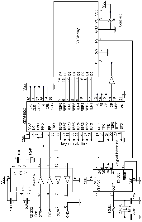
Our LCD needs parallel data, so we have attached the LCD to our serial to parallel interface that we previously designed:
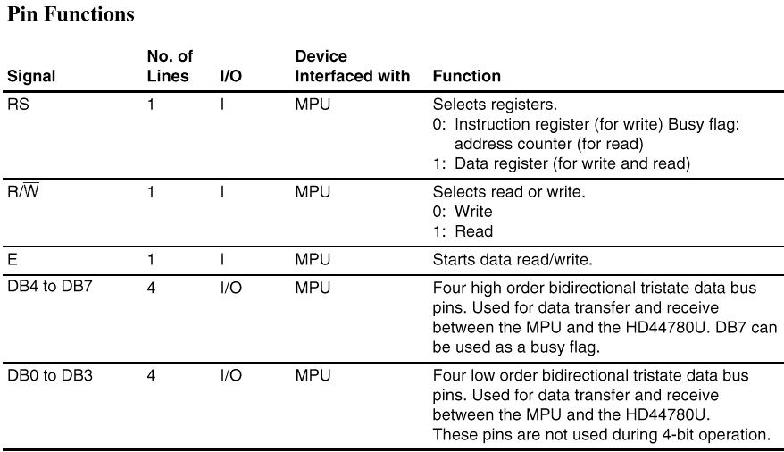
- Pin Functions

6.0.1
The Register Select Pin
The RS pin determines whether the byte on the data lines (DB7-DB0) is an instruction or a byte of data. This pin must be low for an instruction and high for data transfer.
Using the serial/parallel interface developed in earlier chapters, the RS pin is controlled by the DTR pin of the serial port. This pin is memory-mapped to the DTR bit of the control register of the serial port, which can be manipulated directly in code. The LCD driver functions LCD_instruction_mode() and LCD_data_mode() do just that.
- The Read / Write Pin
As implied by its name, the R/W pin selects read from or write to the LCD.
With the serial/parallel interface, this pin is grounded. We have found little use for reading from the LCD, and thusly discarded this feature.
The Enable Pin
One of the more important pins of the LCD, the enable pin signals the LCD to begin functioning. Given the inherent delay in the LCD controller chip, it is necessary that the E pin remain high for a certain time period, which varies for each instruction or datum (these values are listed in the table below).
With the serial/parallel interface, this pin is controlled by the Xilinx FPGA. The FGPA waits until a complete byte is ready for the LCD, which it then places on the data lines and asserts the E pin for the LCD. Instead of calculating the required time for each instruction, the Xilinx simply holds the E pin high for a constant time with every byte. The time period was chosen to be longer than any required time interval. The result is that the operation of the LCD is slightly delayed, but this delay is small enough that it goes unnoticed.
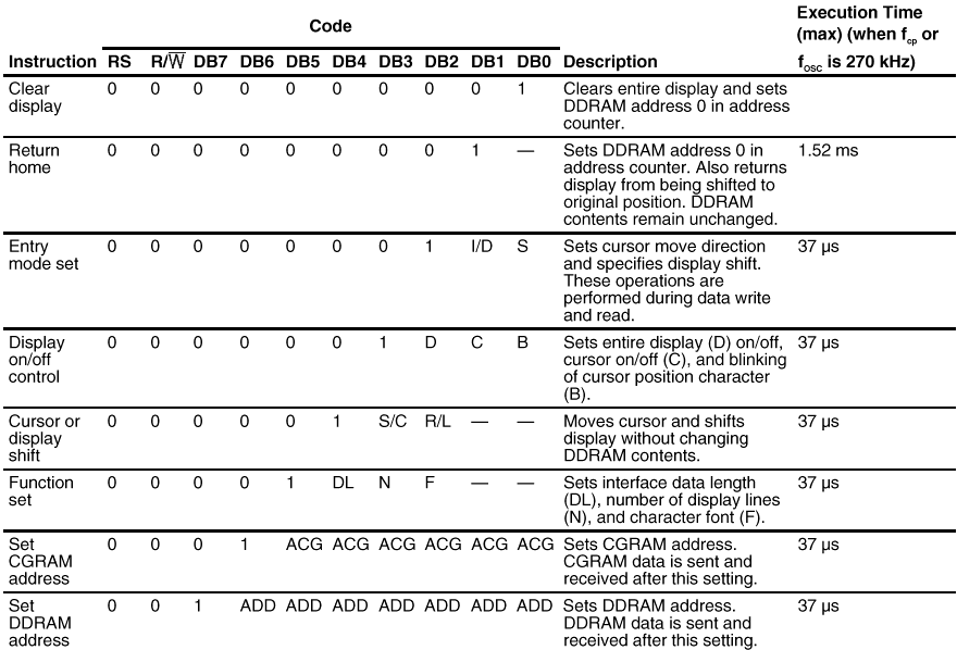
- Instruction Set
- The API
The LCD API contains the following functions
- LCD_instruction_mode() � set the LCD into instruction mode
- LCD_data_mode() � set the LCD into data mode
- LCD_write() � write a byte to the LCD
- lcd_Do() � perform an LCD command
- lcd_WriteChar() � write a character to the LCD (data only)
- lcd_WriteString() � write a string to the LCD
- lcd_SetCursor() � set the LCD cursor to blink, underscore, or off.
- lcd_Initialize() � initial the LCD data structure
The lcd_Do() command can be used in conjunction with defined mnemonics to access the entire LCD function set. For example, to clear the display, one could use the function
lcd_Do(lcd_Clear_Display);
Every function of the LCD has a defined mnemonic and can be accessed this way (please see the code for a complete listing).
6.3 References
How to control HD44780-based Character-LCD, http://home.iae.nl/users/pouweha/lcd.htm.
7.1 Objective
This application note describes the design used to interface a 4x4 keypad to the IBM 403GCX via a serial port.
7.2 Overview
The 403GCX has very little connectivity in comparison to other PowerPC evaluation boards. The main connections on the board include two serial ports and an ethernet port. The 403GCX does not have any traditional monitor output or keyboard input ports, so its usefulness is somewhat one-dimensional.
One use for the evaluation board includes interfacing with a four row, four column keypad. This application note describes two facets of the keypad interface design�the software and hardware perspectives of the design. The software portion of the design involves writing appropriate drivers for the serial port so that data can be read in from the keypad. For the hardware portion of the design, the keypad must utilize several hardware components in order to function properly with the serial port.
7.3 Hardware Design
Block Diagram with Serial to Parallel Interface: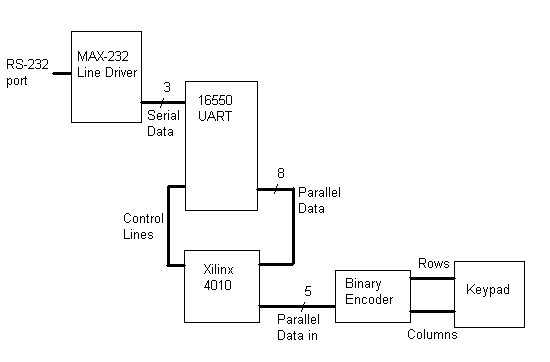
In designing the hardware, several key issues must be confronted. The keypad data must be converted into a format that the serial port can understand. This is done with several key components. They are outlined as follows:
- 16 Key to Binary Encoder
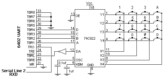
The 74C922 is a 16 key to binary encoder. This IC is responsible for debouncing the keypad and encoding the keypad data. Debouncing the data is important because, with the fast clock, the keypad will output several iterations of each key pressed. The debouncer circuit will insure that only one key was pressed, even though the keypad output will suggest otherwise.
The 74C922 also has a data available line, which goes high whenever a key is pressed on the keypad. This can be used to signal when data is ready for the UART.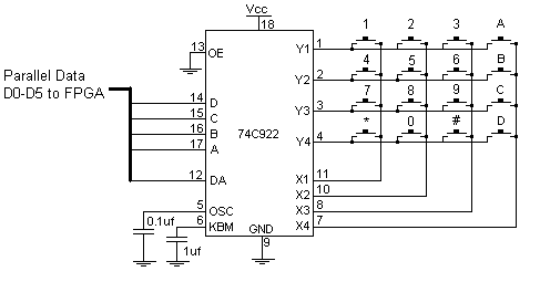
- The Keypad
The keypad being used in this design is a 4x4 keypad. The keypad is driven by the 16 key to binary encoder.
7.4 Overview of Software Design
The software design consists of initializing the interrupts so that the interrupt is active and the appropriate interrupt handler is called. The libraries included with the High C compiler make this task easy. However, understanding of the functionality of these libraries is essential to programming interrupt-driven events.
For the keypad, the interrupt initialization involves a number of settings. The priority level of intterupts on DMA channels, serial port, JTAG port, and external interrupt pins is level 16. This can be seen in Table 4.1.

Table 4.1: Interrupt/Exception Priorities
When an interrupt on this level is detected, the interrupt level is compared to the current task. If the current task has a higher priority, it is handled before the keypad interrupt is called.
Upon calling the interrupt handler, the Save/Restore Register 0 (SRR0) stores the address of the next instruction to be processed. Save/Restore Register 1 stores the current value of the Machine State Register (MSR). The MSR is then updated to reflect the current state. The bits of the MSR are seen in Table 4.2.

Table 4.2 Machine State Register Bit Field
Next, the address of the interrupt handler is determined by concatenating the high-order 16-bits of the Exception Vector Prefix Register (EVPR) and the exception vector offset, seen in Table 4.3. For an external interrupt (such as the serial port interrupt used with the keypad), the offset is 0500.

Table 4.3 Exception Vector Offsets
After the interrupt is called, an rfi (return from interrupt) instruction invokes the contents of SRR0 to be copied into the program counter, and SRR1 into the MSR. Execution then resumes at the address of the program counter.
- The Machine State Register
The Machine State Register (MSR) holds the current state of the 403GCX evaluation board. Several of its bits must be set to appropriately identify and execute an interrupt. The Wait State Enable bit (bit 13) must be set to 1 so that the MSR handles interrupts. Also, bit 16 (External Interrupt Enable) must be set to 1 to handle asynchronous exceptions.
- The Exception Vector Prefix Register (EVPR)
The EVPR stores a 16-bit prefix for the interrupt handler location. This register stores a 16-bit address in its high-order 16-bits. When an interrupt handler is called, the high-order bits of the EVPR are concatenated with the exception vector offsets (Table 4.3) to form the memory address of the interrupt.
- External Interrupt Enable Register (EXIER)
The EXIER contains enable bits for the different types of external interrupts. The EXIER enables these different bits in order to handle various interrupts. Table 4.4 shows the bits of the EXIER. The Serial Port Interrupt Enable bit (bit 4) should be set high to enable serial port receiver interrupts. If the keypad is connected to the JTAG serial port, then the JTAG Serial Port Receiver Interrupt Enable bit (bit 6) must be set high. Finally, the External Interrupt X Enable bits (bits 27 through 31) enable interrupt X, where X is an integer between 0 and 4. All other bits can be set low to disable those types of interrupts.

Table 4.4 External Interrupt Enable Register Bit Field
7.4.4 The External Interrupt Status Register (EXISR)
The EXISR contains the status of the five external interrupts, the DMA channel interrupts, and the JTAG and regular serial port interrupts. This register can be used to check the status of the various interrupts. The bits of this register can be seen in Table 4.5.

Table 4.5 External Interrupt Status Register Bit Field
7.5 Tying It All Together�The Actual Code
Interrupts require configuration of several key registers. However, with the built-in libraries included with the High C Compiler and 403GCX tools, interrupt handlers can be written from a higher level of abstraction using C. The following functions can be used to initialize and handle external interrupts, such as those used for the keypad.
7.5.1 The FLIH_T struct
This struct stores information relative to the interrupt handler. The definition of the struct is as follows:
typedef struct flih_t {
void *flih_stack;
void *flih_function;
void *arg;
}
The flih_stack variable points to a 16-byte alligned stack which should have memory allocated. The flih_function variable is a pointer to the function which handles the interrupt. Finally, the arg variable is a pointer to a list or arguments to be passed to the interrupt handler function.
- ext_int_config(int event, int flags)
This function configures the interrupt type. Basically, it takes an interrupt of priority event (in the case of the keypad, event is 16) and initializes it to the values of flags, which allow the interrupt to be set as edge triggered, as well as negative active or positive active.
- ext_int_enable(int event)
This function enables the interrupt of priority event. For the keypad, event should be 16.
- ext_int_install(int event, flih_t *new_flih, flih_t *old_flih)
This function sets the first level interrupt handler for the interrupt by assigning a flih_t struct for the interrupt of level event (for the keypad, event is 16). If new_flih is NULL, it removes the existing flih_t struct for the interrupt. If old_flih is not NULL, it stores the old first level interrupt handler for the interrupt in the structure pointed to by old_flih.
- ext_int_query(int event, flih_t *flih)
This function stores to existing values of the first level interrupt into the struct pointed to by flih for interrupt level event.
- Ext_int_disable(int event)
This function disables the interrupt of level event.
- The Actual Code
The following is actual code used for the interrupt handler. This can be used as a skeleton for designing the actual interrupt handler.
#include <ioLib.h>
#include <flih.h>
#include <stdio.h>
#include <stdlib.h>
void *inthandle()
{
;
}
main()
{
flih_t fliht;
void *fpinthandle;
fpinthandle=(void *)inthandle;
fliht.flih_function=fpinthandle;
fliht.arg=NULL;
fliht.flih_stack=malloc(4096);
ext_int_install(16, fliht, NULL);
ext_int_config(16, 0);
ext_int_enable(16);
return(0);
}
For this code, the function inthandle is the function called when an interrupt is found of priority 16. Within the main section of this code, fliht�s variables are set to the function handler via a function pointer. The stack is initialized with malloc(). Then, the fliht struct is assigned to the interrupt via the ext_int_install() function. Next, the ext_int_config() function can adjust the functionality of the interrupt so that the interrupt coincides with the hardware design. Finally, ext_int_enable() enables the interrupt of level 16.
The included header files are utilized by the functions discussed above.
7.6 References
PPC403GCX Embedded Controller User�s Manual, http://www.chips.ibm.com/products/powerpc/chips/gcx_um.pdf.
Using VxWorks
Serial / Parallel Converter Circuit w/ Keypad and LCD
|
Pin Number |
Abbr. |
Full Name |
Notes |
|
Pin 1 |
VDD |
+ 5v Supply Rail |
|
|
Pin 2 |
NC |
Not Connected |
|
|
Pin 3 |
GND |
Ground |
|
|
Pin 4 |
RRD |
Receiver Register Disable |
When driven high, outputs RBR8:RBR1 are High Impedance. |
|
Pin 5:12 |
RBR8:
RBR1 |
Receiver Buffer Register |
Receiver's Data Bus |
|
Pin 13 |
PE |
Parity Error |
When High, A Parity Error Has Occurred. |
|
Pin 14 |
FE |
Framing Error |
When High, A Framing Error Has Occurred. i.e. The Stop Bit was not a Logic 1. |
|
Pin 15 |
OE |
Overrun Error |
When High, Data has been received but the nData Received Reset had not yet been activated. |
|
Pin 16 |
SFD |
Status Flag Disable |
When High, Status Flag Outputs (PE, FE, OE, DR and TBRE) are High Impedance |
|
Pin 17 |
RRC |
Receiver Register Clock |
x16 Clock input for the Receiver Register. |
|
Pin 18 |
nDRR |
Data Received Reset |
Active Low. When low, sets Data received Output Low (i.e. Clears DR) |
|
Pin 19 |
DR |
Data Received |
When High, Data has been received and placed on outputs RBR8:RBR1. |
|
Pin 20 |
RRI |
Receiver Register In |
RXD - Serial Input. Connect to Serial Port, Via RS-232 receiver. |
|
Pin 21 |
MR |
Master Reset |
Resets the UART. UART should be reset after applying power. |
|
Pin 22 |
TBRE |
Transmitter Buffer Register Empty |
When High, indicates that Transmitter Buffer Register is Empty, thus all bits including the stop bit have been sent. |
|
Pin 23 |
nTBRL |
Transmitter Buffer Load / Strobe |
Active Low. When low, data present on TBR8:TBR1 is placed in Transmitter Buffer Register. A Low to High Transition on this pin, then sends the data. |
|
Pin 24 |
TRE |
Transmitter Register Empty |
When High, Transmitter Register is Empty, thus can accept another byte of data to be sent. |
|
Pin 25 |
TRO |
Transmitter Register Out (TXD) |
TXD - Serial Output. Connect to Serial Port, Via RS-232 Transmitter. |
|
Pin 26:33 |
TBR8:
TBR1 |
Transmitter Buffer Register |
Data Bus, for Transmitter. Place Data here which you want to send. |
|
Pin 34 |
CRL |
Control Register Load |
When High, Control Register (PI, SBS, CLS2, CLS1, EPE) is Loaded. Can be tied high, so changes on these pins occur instantaneously. |
|
Pin 35 |
PI |
Parity Inhibit |
When High, No Parity is Used for Both Transmit and Receive. When Low, Parity is Used. |
|
Pin 36 |
SBS |
Stop Bit Select |
A High selects 2 stop bits. (1.5 for 5 Character Word Lengths) A Low selects one stop bit. |
|
Pin 37:38 |
CLS2:
CLS1 |
Character Length Select |
Selects Word Length. 00 = 5 Bits, 01 = 6 Bits, 10 = 7 Bits and 11 = 8 Bits. |
|
Pin 39 |
EPE |
Even Parity Enable |
When High, Even Parity is Used, When Low, Odd Parity is Used. |
|
Pin 40 |
TRC |
Transmitter Register Clock |
16x Clock input for Transmitter. |
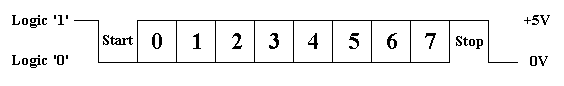 Serial transmission